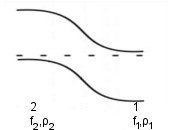
Quantum wells and heterojunctions
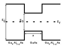
If we put two undoped semiconductors together, the chemical potential must be continuous across the junction- this creates a heterojunction. Two such junctions can be put together to form a quantum well.
In reality, this is a finite potential well, but we’ll treat it as an infinite one to make the maths easier.
Infinite potential well:
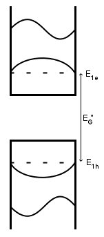 Electrons have energy levels
Holes have energy levels 
We now have an effective band gap EG’’=EG+E1e+E1h.
As we have confinement in one dimension, the system looks two-dimensional (when E2-E1>kT).
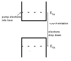
We get peaks in the absorption where there are transitions between two energy levels. As the well widens, the energy levels get closer and the absorption tends to the 3D absorption curve drawn earlier.
Quantum well laser: the laser transition is E1 electrons to E1 holes (these are the most populated levels, unsurprisingly). Quantum well lasers are used in fibre optic communications, CD players and laser pointers.
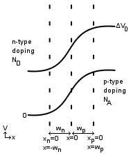
pn junction
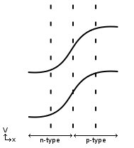
Once again the chemical potential must be continuous across the junction. Say the potential across the gap

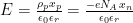
In the central region, electrons and holes annihilate to produce a depletion layer of low carrier density (ionised impurities are still present). There is a net E-field in this region.
pn junctions are massively useful.
Depletion layer: pn junction, area A.
Potential across junction
Boundary conditions: E=0 at the edges of the depletion layer; E, V continuous at x=0 (xn=wn, xp=-wp)
Charge density on p-side

Charge density on n-side


Integrate and use boundary conditions to get
–wn<x<0

0<x<wp
At x=0, the E-field must be continuous, so NDwn= NAwp
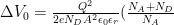
Potential across depletion layer

–wn<x<0

0<x<wp

V must also be continuous at x=0
\frac{eN_Dx_n^2}{2\epsilon_0 \epsilon_r} =\frac{-eN_Ax_p^2}{2\epsilon_0 \epsilon_r}+\frac{E_G}{e}$
If ND=NA, wn=wp=δ, and the depletion layer has width 2δ
In this case


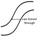
δ~10-6m
If δ is small, then tunnelling can occur.
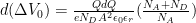
Capacitance of a pn junction
Total stored charge Q=eNDwnA

But recall that

So
So 
Usually, C≈100pF
Stored charge due to excess minority carriers on one side of a pn junction.
Continuity equation: rate of loss of carriers=recombination rate + outflow of carriers

(for these purposes, J is a number current)
But 
In the steady state,


Define a diffusion length


At, x=0, 
Total carrier number

Total stored charge
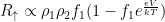
pn junction with an applied bias (Ebers-Moll equation)
No bias
Fermi Golden Rule
right -> left
left -> right
If f1=f2, these are identical and there is no net current.
Apply a bias (voltage) across the junction.
Raise energy levels on RHS
Now 

These rates are proportional to the current I.
Total
![I \propto [f_1(1-f_1 e^{\frac{eV}{kT}})-(1-f_1)f_1 e^{\frac{eV}{kT}}]](https://s0.wp.com/latex.php?latex=I+%5Cpropto+%5Bf_1%281-f_1+e%5E%7B%5Cfrac%7BeV%7D%7BkT%7D%7D%29-%281-f_1%29f_1+e%5E%7B%5Cfrac%7BeV%7D%7BkT%7D%7D%5D&bg=ffffff&fg=000000&s=0&c=20201002)
![I \propto f_1-f_1^2 e^{\frac{eV}{kT}}-f_1 e^{\frac{eV}{kT}}+f_1^2 e^{\frac{eV}{kT}}]](https://s0.wp.com/latex.php?latex=I+%5Cpropto+f_1-f_1%5E2+e%5E%7B%5Cfrac%7BeV%7D%7BkT%7D%7D-f_1+e%5E%7B%5Cfrac%7BeV%7D%7BkT%7D%7D%2Bf_1%5E2+e%5E%7B%5Cfrac%7BeV%7D%7BkT%7D%7D%5D&bg=ffffff&fg=000000&s=0&c=20201002)
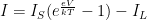
![I=I_0[1- e^{\frac{eV}{kT}}]](https://s0.wp.com/latex.php?latex=I%3DI_0%5B1-+e%5E%7B%5Cfrac%7BeV%7D%7BkT%7D%7D%5D&bg=ffffff&fg=000000&s=0&c=20201002)
Solar cell: forward biased pn junction.
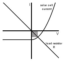
The shaded box represents the power output of the solar cell.
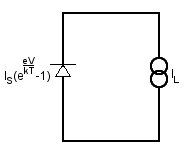
The solar cell has a total current
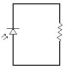
Looks like a diode and a constant current source.
Einstein relation
Electrons

Holes

The D‘s are just diffusion constants.
Potential across a pn junction (revisited)
Start by thinking about total currents (be careful of sign conventions in this section)
Electrons
and similarly for holes.
In equilibrium, J=0


(we get the limits by remembering that on the n-side, 

Integrate to get
pn junction breakdown at large reverse bias can occur in two ways:
- Tunnelling: a valence electron in the p-region makes a transition to the conduction band of the n-region. Tunnelling requires ND, NA ~5×10²³ m-1 -> E > 108 Vm-1
- Avalanche: a thermally generated electron gains enough kinetic energy in the E-field to cause impact ionisation in which an electron-hole pair is generated. Multiplication factors of ~100 can be achieved with several hundred volts of reverse bias.
Photodiodes are used to measure optical signals. There are two modes of operation.
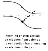
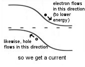
- Photovoltaic mode: photons with hν>EG generate electron-hole pairs in a pn junction. Electrons are swept to the positively charged n region and holes to the negatively charged p region, reducing the voltage below its equilibrium value.
Current generated by a beam of light, power P, photon energy hν

New drift current=I0+IP
To maintain equilibrium, diffusion current must also increase.
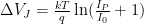
Change in junction voltage is ΔVJ
Diffusion current is now


- Photoconductive mode: a reverse bias is applied to the junction, reducing the drift and diffusion currents and increasing the width of the depletion layer. If photons are now absorbed in the depletion layer, a ‘generation’ current is produced which is proportional to the absorbed power.
Sensitivity

η~0.8, R0~0.55 AW-1
We can improve the sensitivity by incorporating a relatively thick intrinsic layer between the two doped regions so that more of the incident light is absorbed. This is a p-i-n diode.
Speed of a photodiode detector depends on
- Drift time of carriers across the depletion layer.
- Diffusion through p and n regions (diffusion is slower than drift, so those layers must be much thinner than the depletion layer).
- RC time constant of the circuit.
Solar cell revisited: current through a solar cell

Open circuit voltage (I=0)

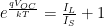
$V_{OC}=\frac{kT}{q}\ln(\frac{I_L}{I_S}+1)$ looks familiar, doesn’t it?
